|
|
|
November 2011:
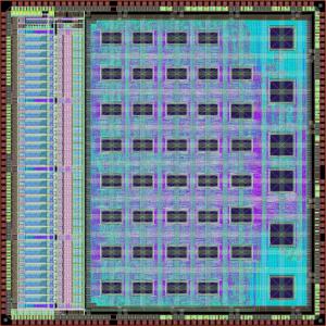
Layout of the SPADIC v 1.0 chip that was submitted on November 6th 2011. The die has a size of 5mm x 5mm. About one-third of the chips is analog, the rest digital. Each mixed mode channel basically consists of two front-ends (switchable), an ADC, an IIR filter, a hit detection logic and a message builder. Via a switch and further on a sophisticated link protocol the message data of the 32 channels is sent out via two 500 Mbps lvds links. The chip works like an oscilloscope: instead of amplitudes pulses as a whole are read out.
|